Xbox One Hardware - more than meets the eye
Xbox One Hardware - more than meets the eye
![]() af cigi silk » 21. jun 2014 23:24
af cigi silk » 21. jun 2014 23:24
Først hørte vi om MS som fortæller om deres FPGA chips i deres server løsninger
http://newsroom.altera.com/press-releas ... center.htm
XBOX one lydchip som er egenudviklet af MS med udgangspunkt i Tensilica som har relationer til Altera som MS har valgt at bruge i deres Server løsninger.
http://www.cadence.com/cadence/newsroom ... _tensilica
http://semiaccurate.com/2013/09/03/xbox ... han-audio/
http://semiaccurate.com/2013/08/30/a-de ... ie-memory/
Hvad er FPGA
In related news, Microsoft recently revealed a "Catapult" project that paired Xeon CPUs with daughter cards loaded with Altera FPGAs. That endeavor reportedly delivered big performance gains in Bing search with relatively little additional power draw. In fact, Catapult was successful enough that Microsoft plans to deploy FPGA-infused servers in its production datacenters early next year. I wouldn't be surprised if those servers had hybrid Xeons onboard.[/quote]
http://techreport.com/news/26656/xeon-h ... a-sidekick
http://research.microsoft.com/apps/vide ... ?id=219486
http://www.theregister.co.uk/2014/06/16 ... as/?page=2
Intels forsøg: Intel’s FPGA announcement is simply palpable desperation
http://www.extremetech.com/extreme/1848 ... ance-boost
Intel isn’t naming any partners for this FPGA effort. Why? Because it likely didn’t exist until the Microsoft news hit the headlines
http://semiaccurate.com/2014/06/20/inte ... speration/
There are no details on the companion chip, but Intel has worked with numerous FPGA providers as part of its Custom Foundry business. It partnered with Tabula and Achronix on 22-nm parts, and with Altera on a 14-nm one. That Altera chip is actually an ARM-based design, but the company behind it has several different FPGA products in its stable.
Microsoft har selv tidligere udtalt at XO er en helt ny arkitektur udviklet mere som En super computer.
http://www.totalxbox.com/74852/features ... -xbox-one/
Kilder:
http://newsroom.altera.com/press-releas ... center.htm
http://research.microsoft.com/apps/vide ... ?id=219486
http://www.convergedigest.com/2014/06/a ... ft-on.html
http://newsroom.altera.com/press-releas ... center.htm
XBOX one lydchip som er egenudviklet af MS med udgangspunkt i Tensilica som har relationer til Altera som MS har valgt at bruge i deres Server løsninger.
http://www.cadence.com/cadence/newsroom ... _tensilica
You might notice that on the right hand side of the diagram there is a coherent connection to the CPU and main memory. If this was a simple audio block there would be no need for CPU coherency, nor the AXI bridge that links everything together. AXI is the ARM bus so why would you put that in an audio unit? Think there is more to this than beeps now?
http://semiaccurate.com/2013/09/03/xbox ... han-audio/
The audio block was completely unique. That was designed by us in-house. It's based on four tensilica DSP cores and several programmable processing engines. We break it up as one core running control, two cores running a lot of vector code for speech and one for general purpose DSP. - See more at: http://www.dailytech.com/Microsoft+Clai ... ycP4g.dpuf
The exact count is a bit nebulous though, Microsoft claims “15 special purpose co-processors” not counting the CPUs and GPUs, eight of which are audio.
http://semiaccurate.com/2013/08/30/a-de ... ie-memory/
Hvad er FPGA
First things first, let’s talk field-programmable gate arrays (FPGA). As the name implies, an FPGA is essentially a blank chip that can be repeatedly reprogrammed after manufacturing. With very few exceptions, every chip inside your computer is hard-coded (at the time of manufacturing) to perform just one set of functions. Your CPU can only do exactly what Intel or AMD designed it to do. You can’t take your CPU and turn it into a GPU. But you can take an FPGA, program it to perform one set of functions (say, graphics), and then reprogram it to handle another type of workload (say, sorting through databases).
The main advantage of an FPGA, other than its customizability, is that it has monstrously high performance. In much the same way that an ASIC is by far the fastest and most efficient way of processing a specific workload (and thus why they’re used for Bitcoin farming), an FPGA is also very fast and efficient. They’re not quite as fast or efficient as ASICs, but what you lose in speed you gain in reprogrammability (again, ASICs are set in stone at manufacturing time).
In related news, Microsoft recently revealed a "Catapult" project that paired Xeon CPUs with daughter cards loaded with Altera FPGAs. That endeavor reportedly delivered big performance gains in Bing search with relatively little additional power draw. In fact, Catapult was successful enough that Microsoft plans to deploy FPGA-infused servers in its production datacenters early next year. I wouldn't be surprised if those servers had hybrid Xeons onboard.[/quote]
http://techreport.com/news/26656/xeon-h ... a-sidekick
http://research.microsoft.com/apps/vide ... ?id=219486
Rather than banking on scaling to many, many more cores, let's take a different path," Microsoft researcher Doug Burger told El Reg. "We think specialization is going to be the next big thing – specializing hardware for different workloads."
http://www.theregister.co.uk/2014/06/16 ... as/?page=2
Intels forsøg: Intel’s FPGA announcement is simply palpable desperation
http://www.extremetech.com/extreme/1848 ... ance-boost
Intel isn’t naming any partners for this FPGA effort. Why? Because it likely didn’t exist until the Microsoft news hit the headlines
http://semiaccurate.com/2014/06/20/inte ... speration/
There are no details on the companion chip, but Intel has worked with numerous FPGA providers as part of its Custom Foundry business. It partnered with Tabula and Achronix on 22-nm parts, and with Altera on a 14-nm one. That Altera chip is actually an ARM-based design, but the company behind it has several different FPGA products in its stable.
the problem with FPGA is they are harder than GPU so MS have to be provide the framework & tools to support it
it is also why HSA also adopts DSP/FPGA not just CPU/GPU generally, DSP/FPGA of X1 audio block for example is just like PS3 Cell , a fusion of SIMD/vector and scalar
Microsoft har selv tidligere udtalt at XO er en helt ny arkitektur udviklet mere som En super computer.
http://www.totalxbox.com/74852/features ... -xbox-one/
This is a effectively a super-computer design," he says. "This is a design out of the super-computer realm. So I expect that we're going to continue to see fairly large improvements in GPU output as people really tune these data sets."
Kilder:
http://newsroom.altera.com/press-releas ... center.htm
http://research.microsoft.com/apps/vide ... ?id=219486
http://www.convergedigest.com/2014/06/a ... ft-on.html
-
cigi silk
- Niveau 5
- Indlæg: 815
- By: Silkeborg
Re: Xbox One Hardware - more than meets the eye
![]() af cigi silk » 22. jun 2014 22:46
af cigi silk » 22. jun 2014 22:46
Positive nyheder for xbox one og anvendelsen af eSram
Yebis 2 Uses Xbox One eSRAM For Buffer, PS4 Unified Architecture Irrelevant Since Yebis Is GPU-Based
Read more at http://gamingbolt.com/yebis-2-uses-xbox ... 9cKXy7T.99
The power disparity from either GPU is by no means that much of a difference. The point he is making is that the GDDR5 is THE main memory for the whole PS4 APU with a unified architecture. ESRAM is specifically a bandwidth feeder for the XOne's GPU, and has more bandwidth given developers use it aside from the conventional method of rendering from the GPU.
Kilde: Yebis http://www.siliconstudio.co.jp/middleware/yebis/en/
YEBIS 2
Optics post effect middleware
-
cigi silk
- Niveau 5
- Indlæg: 815
- By: Silkeborg
Re: Xbox One Hardware - more than meets the eye
![]() af hackNICE1112@ » 23. jun 2014 05:13
af hackNICE1112@ » 23. jun 2014 05:13
cigi silk skrev:Positive nyheder for xbox one og anvendelsen af eSram
Yebis 2 Uses Xbox One eSRAM For Buffer, PS4 Unified Architecture Irrelevant Since Yebis Is GPU-Based
Read more at http://gamingbolt.com/yebis-2-uses-xbox ... 9cKXy7T.99
The power disparity from either GPU is by no means that much of a difference. The point he is making is that the GDDR5 is THE main memory for the whole PS4 APU with a unified architecture. ESRAM is specifically a bandwidth feeder for the XOne's GPU, and has more bandwidth given developers use it aside from the conventional method of rendering from the GPU.
Kilde: Yebis http://www.siliconstudio.co.jp/middleware/yebis/en/
YEBIS 2
Optics post effect middleware
Spænden
-
hackNICE1112@
- Niveau 5
- Indlæg: 1258
Re: Xbox One Hardware - more than meets the eye
![]() af cigi silk » 24. jun 2014 08:01
af cigi silk » 24. jun 2014 08:01
Det betyder at Yebis som er et middelware selskab som laver post processing effects har fundet en model til at lade det hele foregå via ESRAM på Xbox One. Med andre ord så vil den ikke have behov for at tilgå DDR3 RAM.
I praksis betyder det så, at ders middleware vil virke bedre og mere effektivt med XBOX one pga. den hurtigere hastighed på Esram og laver latency.
Du skulle i øvrigt se hvad de laver - det ser virkelig fedt ud . Bl.a. Final Fantasy XV, Destiny Warrior bruger Yebis.
I praksis betyder det så, at ders middleware vil virke bedre og mere effektivt med XBOX one pga. den hurtigere hastighed på Esram og laver latency.
Du skulle i øvrigt se hvad de laver - det ser virkelig fedt ud
-
cigi silk
- Niveau 5
- Indlæg: 815
- By: Silkeborg
Re: Xbox One Hardware - more than meets the eye
![]() af cigi silk » 30. jun 2014 09:30
af cigi silk » 30. jun 2014 09:30
Her er et linkt til sidste powerpoint præsnetatin som MS og AMD holdt i Stokholm 2. juni-2014.
http://amd-dev.wpengine.netdna-cdn.com/ ... r_new.ppsx
Det afgørende er at de skriver - at der stadig er NDA (ting som de ikke må sige) - som overskriften siger ... More than meets the eye
Som de skriver:
This is a non NDA event, to there is a limit to how much I can say, go easy!
Omkring audio delen:
Costom audio hardware
Lots of features
Kinda cool!
Nuff said
..... medandre ord - der er noget omkring audio chippen som de ikke ønsker at gå i detaljer men!
Det matcher de tidlgiere indlæg omkring audio chippen er meget mere end audio.
-
cigi silk
- Niveau 5
- Indlæg: 815
- By: Silkeborg
Re: Xbox One Hardware - more than meets the eye
![]() af cigi silk » 2. jul 2014 07:56
af cigi silk » 2. jul 2014 07:56
Nu begynder der stille og rolig at blive åbnet op for posen.

Intel er nu begyndt at bruge det setup som forventes allerede at ligge i XO.
Intel bruger stacked memory(se nedenfor), FPGA (Tensilixa i Xbox One - har jeg skrevet om tidligere),noc (network on a chip - er også tidliger nævnt). Se i øvrigt relationen til Micron som er en del af MS samarbejde.
http://www.bit-tech.net/news/hardware/2 ... hmc-tech/1
Min forventning er at nedenstående allerede er blevet prototypet i XBOX one - det som tidligere var forventning om var stacked GPU, er stacked Memory, mens Tensilica audio chippen i stedet er det som er tænkt til offloading af compute.
MS egen forskning
http://research.microsoft.com/apps/mobi ... ?id=217166
I slutningen af deres skriv henviser de til Doug Burger, som også er nøgle personen i FPGA udviklingen på server løsninger, og XBox one.
http://cag.engr.uconn.edu/isca2014/program.html
Keynote I: Insight into the MICROSOFT XBOX ONE Technology
Chair: Doug Burger, Microsoft
Intel er nu begyndt at bruge det setup som forventes allerede at ligge i XO.
Intel bruger stacked memory(se nedenfor), FPGA (Tensilixa i Xbox One - har jeg skrevet om tidligere),noc (network on a chip - er også tidliger nævnt). Se i øvrigt relationen til Micron som er en del af MS samarbejde.
http://www.bit-tech.net/news/hardware/2 ... hmc-tech/1
Min forventning er at nedenstående allerede er blevet prototypet i XBOX one - det som tidligere var forventning om var stacked GPU, er stacked Memory, mens Tensilica audio chippen i stedet er det som er tænkt til offloading af compute.
The Hybrid Memory Cube Consortium, a group of memory industry giants led by Micron and Samsung, has announced a new member: software behemoth Microsoft.
The Hybrid Memory Cube (HMC) technology espoused by the group is a planned implementation of through-silicon via (TSV) technology - vertical conduits through a chip's silicon infrastructure which allows components to be placed in a three-dimensional mesh rather than in a traditional planar manner - which promises to dramatically improve the performance of future memory modules.
Prototypes shown off by Micron earlier this year have already proved more than capable of taking over from traditional DRAM components, showing peak throughput of 128GB/s compared to the 12.8GB/s from commercial-grade DDR3 modules created on a planar process.
It's not all about performance, however: the process also promises dramatic power savings for mobile gadgets, with Micron's prototype modules showing a 70 per cent reduction in power draw during data transfer in a module one-tenth the size of current-generation technologies.
The technology is impressive enough to have won a stack of awards, including the Linley Group's Best New Technology Award in its 2011 round-up. Thus far, however, it is notable in its absence from the commercial markets. While there is no timescale available on when the product may launch, the fact that Microsoft is showing an interest suggests it's not too far away from becoming a commercial reality.
'HMC technology represents a major step forward in the direction of increasing memory bandwidth and performance, while decreasing the energy and latency needed for moving data between the memory arrays and the processor cores,' claimed Microsoft's general manager of strategic software/silicon architectures KD Hallman in an announcement to press. 'Harvesting this solution for various future systems could lead to better or novel digital experiences.'
MS egen forskning
http://research.microsoft.com/apps/mobi ... ?id=217166
A High Memory Bandwidth FPGA Accelerator for Sparse Matrix-Vector Multiplication Read the publication
Jeremy Fowers, Kalin Ovtcharov, Karin Strauss, Eric Chung, and Greg Stitt, in International Symposium on Field-Programmable Custom Computing Machines, IEEE [May 2014]
Sparse matrix-vector multiplication (SMVM) is a crucial primitive used in a variety of scientific and commercial applications. Despite having significant parallelism, SMVM is a challenging kernel to optimize due to its irregular memory access characteristics. Numerous studies have proposed the use of FPGAs to accelerate SMVM implementations. However, most prior approaches focus on parallelizing multiply-accumulate operations within a single row of the matrix (which limits parallelism if rows are small) and/or make inefficient uses of the memory system when fetching matrix and vector elements. In this paper, we introduce an FPGA-optimized SMVM architecture and a novel sparse matrix encoding that explicitly exposes parallelism across rows, while keeping the hardware complexity and on-chip memory usage low. This system compares favorably with prior FPGA SMVM implementations. For the over 700 University of Florida sparse matrices we evaluated, it also performs within about two thirds of CPU SMVM performance on average, even though it has 2.4x lower DRAM memory bandwidth, and within almost one third of GPU SVMV performance on average, even at 9x lower memory bandwidth. Additionally, it consumes only 25W, for power efficiencies 2.6x and 2.3x higher than CPU and GPU, respectively, based on maximum device power.
I slutningen af deres skriv henviser de til Doug Burger, som også er nøgle personen i FPGA udviklingen på server løsninger, og XBox one.
We would like to thank Doug Burger and the Catapult team for their support and help with this project. We would
also like to thank Adrian Macias from Altera for helping with the accumulator implementation.
http://cag.engr.uconn.edu/isca2014/program.html
Keynote I: Insight into the MICROSOFT XBOX ONE Technology
Chair: Doug Burger, Microsoft
-
cigi silk
- Niveau 5
- Indlæg: 815
- By: Silkeborg
Re: Xbox One Hardware - more than meets the eye
![]() af Niculla » 2. jul 2014 13:43
af Niculla » 2. jul 2014 13:43
(Hvis vi antager at FPGA er en del af X1)
Ved man hvor let det er at omstille sig til at lave spil med FPGA-princippet?
Som det er nu tager CPU'erne tasks i kronologisk rækkefølge. Man må formode at det bliver en del sværere, når de skal angive grænser indenfor CPU'en til parallelle processer i et så hastigt tempo som grafik kræver? Det må kræve en hel del bedre planlægning af de tasks som der skal udføres.
Men det giver god mening, at man med FPGA-princippet kan angive grænser og andele af beregninger til servere i clouden også.
Det hele handler jo bare om at det ikke skal være meget mere besværligt for udviklerne, hvis det rent faktisk skal gøre X1 bedre i praksis.
-
Niculla
- Niveau 3
- Indlæg: 267
- By: Roskilde
Re: Xbox One Hardware - more than meets the eye
![]() af cigi silk » 2. jul 2014 14:18
af cigi silk » 2. jul 2014 14:18
FPGA -Field Programmable Gate Arrays (FPGAs) are semiconductor devices that are based around a matrix of configurable logic blocks (CLBs) connected via programmable interconnects. FPGAs can be reprogrammed to desired application or functionality requirements after manufacturing.
http://www.xilinx.com/training/fpga/fpg ... -array.htm
Det afgørende er her at MS kan offloade "fixed functions", fx. AI, lightring, dynamic weather ( FH2 anyone ) til at blive varetaget af hardware, som er ca. 20 -100 gange hurtigere end en software løsning.
http://www.eetimes.com/document.asp?doc_id=1280560
Som det helt rigtigt fremgår er det afgørende at kodningen af dette kan foregå optimalt og så effektivt for udviklerne som muligt.
Det er derfor ikke uden grund at vi har set MS rykke voldsomt på udviklingsværktøjer C++AMP og ikke mindst DX12.
Det er samtidig derfor vi stadig ikke har set skyggen af det som Xbox one er i stand til. Det fede er så, at MS kan udvikle konsollen løbende ved at forbedre softwaren - så når visse internet personer siger man ikke kan forbedre hardware med software læs drivere dx12 tager de mere fejl end de selv tror.
http://www.xilinx.com/fpga/index.htm
http://www.xilinx.com/training/fpga/fpg ... -array.htm
Det afgørende er her at MS kan offloade "fixed functions", fx. AI, lightring, dynamic weather ( FH2 anyone
FPGAs are a complimentary, semi-custom, co-processing resource that is "picking off" the parallelizable tasks from CPUs. FPGAs do this – at lower clock speeds and power – by deploying multi-core parallelism.
HPRC (High Performance Reconfigurable Computing) as a branch of Computer Science is thriving. Largely driven by GPGPU (general-purpose graphics processing unit) growth, HPRC is also supported by FPGA-based applications. The programming environment is considered to be the main obstacle preventing FPGAs from being used to their full potential in accelerators.
http://www.eetimes.com/document.asp?doc_id=1280560
Som det helt rigtigt fremgår er det afgørende at kodningen af dette kan foregå optimalt og så effektivt for udviklerne som muligt.
Det er derfor ikke uden grund at vi har set MS rykke voldsomt på udviklingsværktøjer C++AMP og ikke mindst DX12.
Det er samtidig derfor vi stadig ikke har set skyggen af det som Xbox one er i stand til. Det fede er så, at MS kan udvikle konsollen løbende ved at forbedre softwaren - så når visse internet personer siger man ikke kan forbedre hardware med software læs drivere dx12 tager de mere fejl end de selv tror.
FPGAs allow designers to change their designs very late in the design cycle– even after the end product has been manufactured and deployed in the field. In addition
http://www.xilinx.com/fpga/index.htm
Senest rettet af cigi silk 2. jul 2014 14:51, rettet i alt 1 gang.
-
cigi silk
- Niveau 5
- Indlæg: 815
- By: Silkeborg
Re: Xbox One Hardware - more than meets the eye
![]() af cigi silk » 2. jul 2014 14:42
af cigi silk » 2. jul 2014 14:42
Faldt lige over den her kommentar som jeg synes rammer det rigtigt godt
http://unionvgf.com/index.php?threads/m ... eath.4696/
Think of it all as nano coding. The philosophy of this is future software paradigm which requires hardware to be designed around it. Much here in line with what MS has said technically behind its cloud infrastructure, X1 design, upcoming (new) DX12 GPUs, etc.. The future is here, just takes time to code it all.
People really fail to realize that MS spends more money on research annually than most of its competitors do put together in the hardware/software space around computing. It's why they (MS) have pretty much just given up explaining themselves and just letting things evolve and show as they come naturally while eventually everyone else will scramble to try to catch up. It is why Intel, AMD and NVidia ate all excited and part of what is coming around the bend; DX12 being a huge part of it all with new GPU architectures built around it. While existing cards will be compliant with DX12, they will not be able to touch new cards built around what DX12 is really about.
It's all related, all next gen technology and software design.
http://unionvgf.com/index.php?threads/m ... eath.4696/
-
cigi silk
- Niveau 5
- Indlæg: 815
- By: Silkeborg
Re: Xbox One Hardware - more than meets the eye
![]() af cigi silk » 5. aug 2014 09:01
af cigi silk » 5. aug 2014 09:01
Her er en lille update omkring hvad MisterC har digget sig frem til - og det ser nu virkelig ud til at begynde at hænge sammen med det som kommer ud af AMD og de tidligere indsiders kommentarer flere år tilbage.
Jeg har valgt at poste det i denne tråd, fordi jeg ikke gider diskutere det med "non-believers" - det er helt op til den enkelte om man ønsker at tro på at MS ikke er idioter og at de har brugt 3 mia til AMD plus egen forskning fornuftigt og på noget som er fremadskuede.
Så hvis man har interesse for hvad der potentielt ligger under hjelmen på Xbox One - så er her noget af det mest gennemarbejdede materiale man kan finde på nettet. Intet er officielt og skal læses mellem linjerne på hvad MS og AMD siger - men som jeg tidligere har skrevet så er vi på vej ind i et helt nyt paradigme som kræver voldsomt meget af driverne og udviklingsværktøjerne (compilerne) for at gøre det effektivt for udviklerne.
Men det bemærkelsesmæsige er at vi allerede nu er ved at have parity med 1080P på langt de fleste store titler, - det var vist en af mine tidligere udsagn at vi efter E3 ville opleve 1080P på nye titler. Og bemærk så at man samtidig kan snappe ting. Ikke dårligt for en 1.3TF maskine mond PS4 1.8TF. Fremtiden handler bare ikke om FLOPS eller ROPS men om at undgå data movement, da det er det som er dyrt og ikke selve compute som er blevet meget billigt - derfor handler det om de rette data det rette sted, og helst lokalt (process in momory / PIM).
De nyeste findings tegner på at MS ikke har 3D stacked GPU som Panella også debunked - men at de har hukommelse potentiel embedded HBM memory som vil være omkring 500-600 GBps - det kan så sammenlignes med PS4 176 MBs max og 135 MBs i praksis.
Part 37. PIM processing in memory
by Mistercteam
Suddenly all fit with X1, AMD recetnly show to the public about their PIM research and so much inline with X1
=======================================================================
A. Reason to go to PIM design, targetted specifically for Supercomputer based arch,
targetted 50 Gflops/w or 25DP Gflops/W
and show basic PIM design, PIM AMD (or MS) design include SIMD + CPU (scalar)

B. PIM in more detail, also AMD tested PIM per block as per 10W wattage
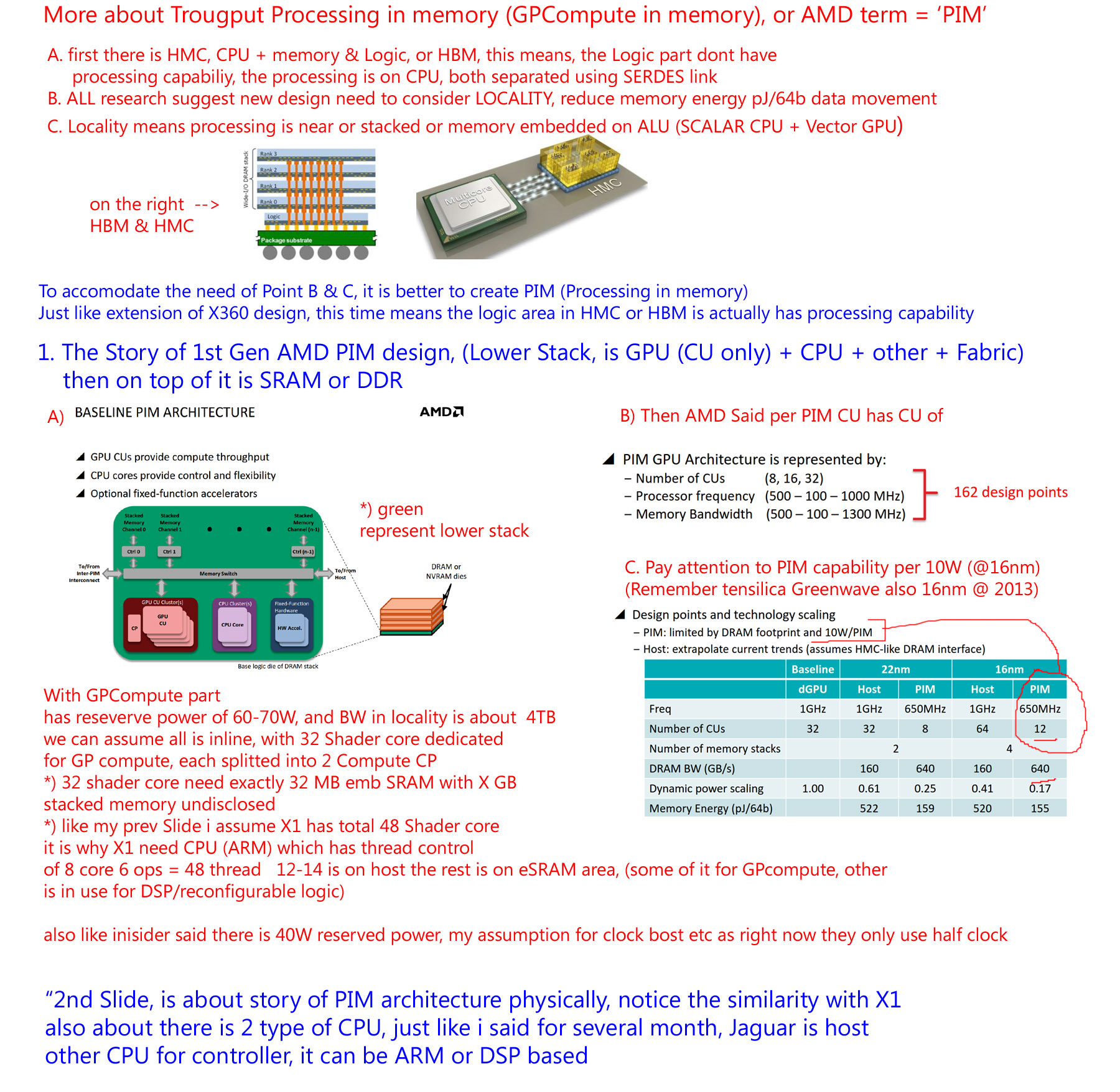
C. PIM physical charateristics, so much inline with X1 hardware layer /eSRAM block
notice that host is not stacked, the only stacked part is PIM block
D. all back to data movement, locality, and also new software stack,
all actually very much inline with X1 May Reveal

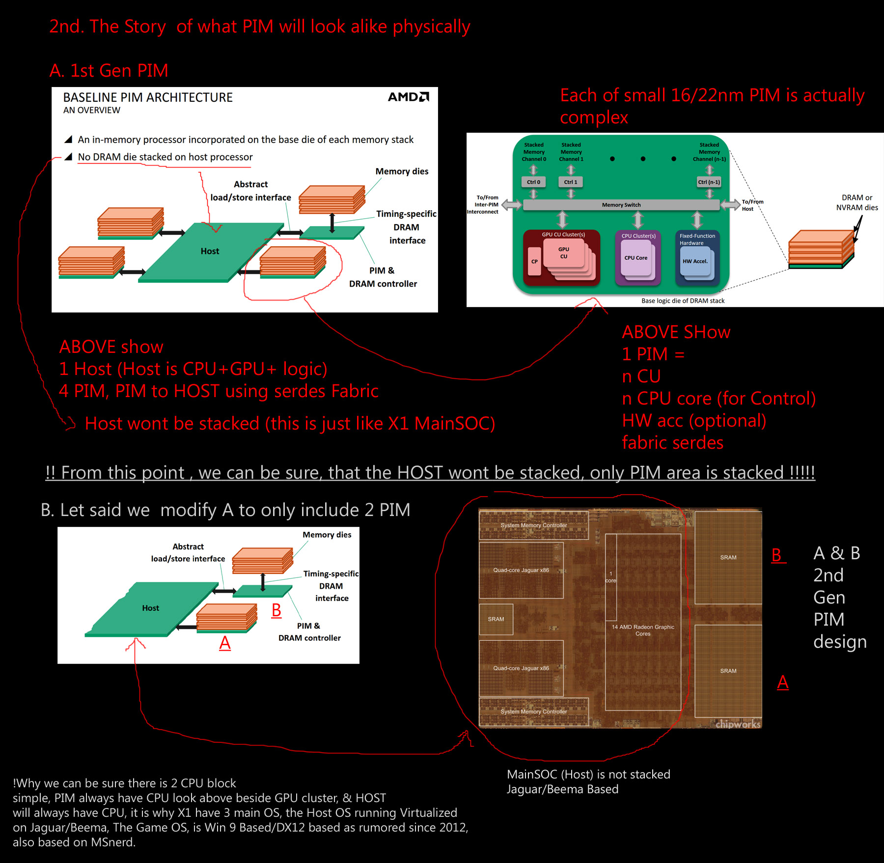
Part 38. PIM design need scratchpad memory
by MIstercteam
Another proof is, ALL PIM design need scratchpad Memory. Very much inline with X1, even with Vgleak
============================================================
Scratch pad memory is less area than cache and more faster and less latency than cache
Jeg har valgt at poste det i denne tråd, fordi jeg ikke gider diskutere det med "non-believers" - det er helt op til den enkelte om man ønsker at tro på at MS ikke er idioter og at de har brugt 3 mia til AMD plus egen forskning fornuftigt og på noget som er fremadskuede.
Så hvis man har interesse for hvad der potentielt ligger under hjelmen på Xbox One - så er her noget af det mest gennemarbejdede materiale man kan finde på nettet. Intet er officielt og skal læses mellem linjerne på hvad MS og AMD siger - men som jeg tidligere har skrevet så er vi på vej ind i et helt nyt paradigme som kræver voldsomt meget af driverne og udviklingsværktøjerne (compilerne) for at gøre det effektivt for udviklerne.
Men det bemærkelsesmæsige er at vi allerede nu er ved at have parity med 1080P på langt de fleste store titler,
- det var vist en af mine tidligere udsagn at vi efter E3 ville opleve 1080P på nye titler. Og bemærk så at man samtidig kan snappe ting. Ikke dårligt for en 1.3TF maskine mond PS4 1.8TF. Fremtiden handler bare ikke om FLOPS eller ROPS men om at undgå data movement, da det er det som er dyrt og ikke selve compute som er blevet meget billigt - derfor handler det om de rette data det rette sted, og helst lokalt (process in momory / PIM).De nyeste findings tegner på at MS ikke har 3D stacked GPU som Panella også debunked - men at de har hukommelse potentiel embedded HBM memory som vil være omkring 500-600 GBps - det kan så sammenlignes med PS4 176 MBs max og 135 MBs i praksis.
Part 37. PIM processing in memory
by Mistercteam
Suddenly all fit with X1, AMD recetnly show to the public about their PIM research and so much inline with X1
=======================================================================
A. Reason to go to PIM design, targetted specifically for Supercomputer based arch,
targetted 50 Gflops/w or 25DP Gflops/W
and show basic PIM design, PIM AMD (or MS) design include SIMD + CPU (scalar)
B. PIM in more detail, also AMD tested PIM per block as per 10W wattage
C. PIM physical charateristics, so much inline with X1 hardware layer /eSRAM block
notice that host is not stacked, the only stacked part is PIM block
D. all back to data movement, locality, and also new software stack,
all actually very much inline with X1 May Reveal
Part 38. PIM design need scratchpad memory
by MIstercteam
Another proof is, ALL PIM design need scratchpad Memory. Very much inline with X1, even with Vgleak
============================================================
Scratch pad memory is less area than cache and more faster and less latency than cache
Senest rettet af cigi silk 5. aug 2014 10:31, rettet i alt 2 gange.
-
cigi silk
- Niveau 5
- Indlæg: 815
- By: Silkeborg
Re: Xbox One Hardware - more than meets the eye
![]() af Jibla » 5. aug 2014 09:36
af Jibla » 5. aug 2014 09:36
Sgu da vildt at man får 720p ud af alle de jpeg billeder!

-
Jibla
- Niveau 7
- Indlæg: 4856

Re: Xbox One Hardware - more than meets the eye
![]() af cigi silk » 5. aug 2014 10:13
af cigi silk » 5. aug 2014 10:13
Konceptet bygger på det her:
http://searchbusinessanalytics.techtarg ... memory-PIM
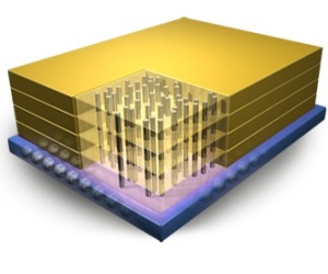
Processing in memory (PIM, sometimes called processor in memory) is the integration of a processor with RAM (usually DRAM or SRAM) on a single chip. The result is sometimes known as a PIM chip.
Processing in memory is one approach to overcoming the von Neumann bottleneck, which is a limitation on throughput caused by the latency inherent in the standard computer architecture. In the standard model, known as the von Neumann architecture, programs and data are held in memory; the processor and memory are separate and data moves between the two. In that configuration, latency is unavoidable. Furthermore, although processor speeds have increased significantly in recent years, memory improvements have mostly been in density – the ability to store more data in less space – rather than transfer rates. As a result, the processor has spent an increasing amount of time waiting for data to be fetched from memory. In effect, a processor is limited to the rate of transfer at the bottleneck.
In PIM chip fabrication, CMOS logic devices and memory cells are tightly coupled; processor logic is directly connected to the memory stack. In effect, the integration of processing and memory increases processing speed and memory transfer rate and decreases latency and power usage.
http://searchbusinessanalytics.techtarg ... memory-PIM
Processing in memory (PIM, sometimes called processor in memory) is the integration of a processor with RAM (usually DRAM or SRAM) on a single chip. The result is sometimes known as a PIM chip.
Processing in memory is one approach to overcoming the von Neumann bottleneck, which is a limitation on throughput caused by the latency inherent in the standard computer architecture. In the standard model, known as the von Neumann architecture, programs and data are held in memory; the processor and memory are separate and data moves between the two. In that configuration, latency is unavoidable. Furthermore, although processor speeds have increased significantly in recent years, memory improvements have mostly been in density – the ability to store more data in less space – rather than transfer rates. As a result, the processor has spent an increasing amount of time waiting for data to be fetched from memory. In effect, a processor is limited to the rate of transfer at the bottleneck.
In PIM chip fabrication, CMOS logic devices and memory cells are tightly coupled; processor logic is directly connected to the memory stack. In effect, the integration of processing and memory increases processing speed and memory transfer rate and decreases latency and power usage.
Senest rettet af cigi silk 5. aug 2014 14:45, rettet i alt 1 gang.
-
cigi silk
- Niveau 5
- Indlæg: 815
- By: Silkeborg
Re: Xbox One Hardware - more than meets the eye
![]() af cigi silk » 5. aug 2014 10:24
af cigi silk » 5. aug 2014 10:24
Jibla skrev:Sgu da vildt at man får 720p ud af alle de jpeg billeder!
Jeg forbløffes hver gang over, at man oplever så tåbelige kommentarer på et XBOX fansite.
-
cigi silk
- Niveau 5
- Indlæg: 815
- By: Silkeborg
Re: Xbox One Hardware - more than meets the eye
![]() af Blauwy » 5. aug 2014 11:03
af Blauwy » 5. aug 2014 11:03
Jibla skrev:Sgu da vildt at man får 720p ud af alle de jpeg billeder!
Cigi, Hvad siger du til at Witcher 3 ikke bliver 1080p selv med DX12?
http://www.gamespot.com/articles/xbox-o ... 0-6421478/
-
Blauwy
- Niveau 7
- Indlæg: 3402
Hvem er online
Brugere der læser dette forum: Ingen og 10 gæster
Xboxlife community
Redaktionen
Entertainment Networks